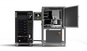
Suitable for wafer-level and panel-level packaging, Photonic Debonding delivers a clean wafer separation solution at a significantly lower cost than lasers.
— Paul Colan, CFO
AUSTIN, TEXAS, UNITED STATES, April 19, 2023/EINPresswire.com/ — PulseForge, Inc. has announced the launch of its latest product, the PD 300 SA semi-automated photonic debonding tool. Designed to enable semiconductor advanced packaging for R&D and low-volume customers, this cutting-edge tool utilizes PulseForge’s patented photonic debonding process. The photonic debonding process leverages high-intensity pulses of light in conjunction with our proprietary, reusable, light-absorbing layer carriers to debond temporarily bonded materials for wafer thinning, hybrid bonding, and micro-LED transfer.
PulseForge Photonic Debonding systems offer a substantially lower cost of ownership than incumbent industry alternatives and provide a clean, ash-free process. Suitable for both wafer-level and panel-level packaging, the PD300 SA is ideal for low-volume and R&D applications. It can debond warped wafers without expensive warpage adjustment hardware or process changes.
“We are thrilled to introduce our patented photonic debonding process to the semiconductor advanced packaging industry,” said Jonathan Gibson, CEO of PulseForge Inc. “We have worked extensively with our material partners and early customers to qualify this technology, and we are confident that it will have a significant impact on the industry. Additionally, we are currently working with multiple solution providers to bring fully automated systems to our customers for high-volume manufacturing environments.”
“PulseForge, Inc. is committed to providing innovative solutions that enable our customers to succeed in today’s fast-paced and demanding manufacturing environments. Our photonic debonding solutions provide improved margins, industrial scale, significantly improved throughput, and shorter lead times for our manufacturing customers,” said Paul Colan, CFO of PulseForge, Inc.
About PulseForge, Inc.
PulseForge, Inc. utilizes applied energy in a precise and targeted manner to enable innovation in industrial manufacturing. Our expertise and tools empower our customers to explore novel materials and manufacturing methodologies, driving dynamic and efficient production at an industrial scale. Learn more at www.pulseforge.com.
Bob Hartline
PulseForge, Inc.
+1 512-439-9195
[email protected]
Visit us on social media:
LinkedIn
Photonic Debonding
![]()
Originally published at https://www.einpresswire.com/article/628796493/pulseforge-launches-semi-automated-photonic-debonding-tool-for-semiconductor-advanced-packaging-industry


